


Products
Search

 Multilayer
1. Introduction
With this product information, we would like to supply you with basic details about the structural options, tolerances, materials and layout guidelines for multilayer boards. This should make your life easier as a developer and help to design your printed circuit boards so that they are optimised for manufacturing at lowest cost.
2. General details
| Standard | Special** | |
|---|---|---|
| Maximum circuit size | 459 x 264 | --- |
| Number of layers | to 24 | On request |
| Pressed thickness | 0.5 mm - 3.2 mm | On request |
3. Materials
As a supplier of prototypes and rush deliveries, CONTAG has a selection of standard materials with which a large bandwidth of the variety of types of PCB can be covered and which are always available in house.
Requirements for other or for special materials can also be met in most cases, but, depending upon the exact requirements, up to about 5 working days may be needed to procure the material.
Do get in touch with us and discuss your needs with one of our sales or CAM team.
Standard materials held in stock:
| Components | Thickness | Tolerance | Weave type |
|---|---|---|---|
| Internal layers | 0,05mm | +/-10% | 106 |
| Internal layers | 0.10mm | +/-10% | 2116 |
| Internal layers | 0,13mm | +/-10% | 1504 |
| Internal layers | 0,15mm | +/-10% | 1501 |
| Internal layers | 0.20mm | +/-10% | 7628 |
| Internal layers | 0,25mm | +/-10% | 2 x 1504 |
| Internal layers | 0.30mm | +/-10% | 2 x 1501 |
| Internal layers | 0.36mm | +/-10% | 2 x 7628 |
| Internal layers | 0,41mm | +/-10% | 2 x 7628 |
| Internal layers | 0,51mm | +/-10% | 3 x 7628/2116 |
| Internal layers | 0,61mm | +/-10% | 3 x 7628 |
| Internal layers | 0.71mm | +/-10% | 4 x 7628 |
| Internal layers | 0,80mm | +/-10% | 4 x 7628/1080 |
| Internal layers | 1,0mm | +/-10% | 5 x7628/2116 |
| Internal layers | 1,2mm | +/-10% | 6 x7628/2116 |
| Internal layers | 1,55mm | +/-10% | 8 x7628 |
| Prepregs | 0.058mm* | Depends on layout | 106 |
| Prepregs | 0.084mm* | Depends on layout | 1080 |
| Prepregs | 0.112mm* | Depends on layout | 2116 |
| Prepregs | 0.205mm* | Depends on layout | 7628 |
* theoretical pressed thickness
Cu thickness for internal layers: Standard - 18µm and 35 µm,
on request 70 µm, 105µm and 140µm
Material type: FR 4
Tg: approx. 150°C
εr at 1 MHz: ≤5,4 (typical: 4,7)
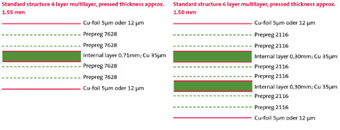
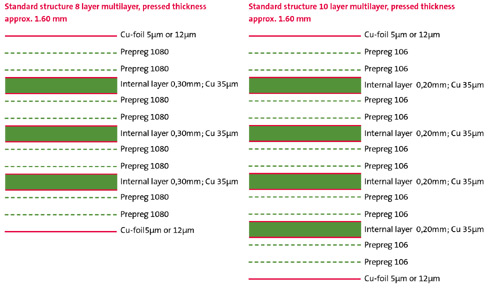
4. Multilayer options
If you do not specify a particular sequence of layers, we will use the following standard sequence for the corresponding number of layers:
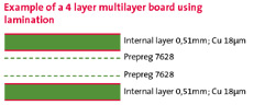
5. Multilayer laminations
If you would like a defined thickness of dielectric between the external layers and the first internal layer, then you can choose this type of construction.
6. Multilayer boards with blind and buried vias
CONTAG can produce multilayer circuit boards with blind and buried vias, even as a rush service. You will find important information and layout hints in our technology information sheet "Blind vias".
7. Design notes
When special layers are requested, we have a simulation programme, with which we can determine the exact insulation spacing, the degree of resin fill and the er value between the individual layers. It is also possible to precisely calculate the final thickness. To do this we need the complete layout for the internal layers.
Basically the following, generally applicable points should be considered for the layers in your boards:
- Plan at least 2 prepreg mats between the layers. (otherwise the resin fill and the insulation may become critical)
- Build up multilayer boards symmetrically. (both for the thickness of the internal layers if you would like to use different core thicknesses, as well as for the prepregs)
- Avoid uneven distribution of Cu on an internal layer. (danger of twisting or warping)
- Note aspect ratio of ¡Ý 1:8. (ratio of smallest drill diameter to pressed thickness)
- The width of pad left after drilling should be at least 0.125 mm around the full circumference. Clearances should be at least 0.30 mm larger than the associated hole diameter. (holes for component leads will be drilled 0.15 mm larger, vias 0.05 mm larger than the final diameter that you specify.)
- Put impedance-controlled tracks on internal layers. (Owing to the close tolerance of the Cu thickness, the cross-section of the tracks is thus more exactly reproducible, the same applies for the restricted tolerance of the thickness of internal layers affecting the dielectric thickness. For dielectric spacing with prepregs, tolerances of ±10% should be used for calculations.)
Talk to our sales team (+49 30 351 788 - 0 or team
 contag.de). We will look together for a functional, optimised and cost-effective solution for your printed circuit boards.
For more detailed technological questions on printed circuit boards, please contact our team of technologists (+49 30 351 788 - 155).
** on request
Version: F
Your personal contact
+49 30 351 788-333
teamcontag.de
 Multilayer product info