


Technologies
Search

 Hole plugging
1. Introduction
Owing to the increasing growth in integration and packing density of electronic circuits, the requirements and the complexity of printed circuit boards are also growing. SBU (sequential build up) multilayer boards with blind and buried vias (see product information on HDI/SBU technology) are of increasing significance here.
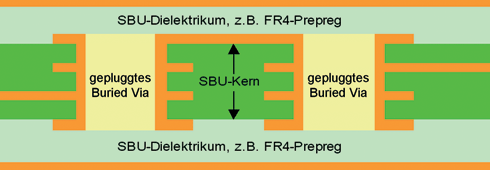
Buried vias in an SBU core, which are not externally visible, form a cavity which is not completely filled by the dielectric when the outside layers are pressed on. This results in depressions in the outer layers appearing, over these hidden holes, which can present a problem for processing.
In addition to this, the location of open, unfilled buried vias cannot be used for a pad for a blind via on the outer layer, which can mean restrictions on the layout of complex circuits. Positioning vias directly in pads is a significant design advantage. If these vias are not closed, then holes that go through the board can result in the solder flowing away, or an air bubble can form in the blind via which can impair the reliability of the solder joint and thus of the entire circuit.
It is thus necessary to completely fill holes, with a planar finish and to possibly also metallise the surface. This technology information sheet is intended to explain the options, procedures and special features of this technology, to help you to optimise your layout and the costs.
2. The resin pastes used
CONTAG uses plugging pastes from the PP 2795 series made by Lackwerke Peters. We mainly use the PP 2795 HV variant, a white, very viscous material.
This paste is distinguished by the following characteristics:
- Solid material content 100%
- Glass transition temperature Tg > 140°C
- Thermal expansion coefficient for temperatures below Tg < 40 ppm/°C
- Meets solderability to IPC-SM-840 C, para. 3.7.2 and MIL - P 55 110C
- V-0 - listed to UL 94
- Solvent-free single component system with minimal volume shrink
- Enables reliable and planar closure of metallised holes
- Good adhesion
- Mills well
- Is excellent for metallisation
3. Technological variants
a) Plugging of buried vias in internal layers or SBU cores to prevent depressions in the outer layers
b) Plugging or buried vias in internal layers or SBU cores and metallisation of the closed holes to use as a pad
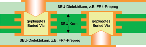
c) Sequential plugging of vias on outer layers and metallisation of the closed holes (via in pad technology)

4. Process description
- Drill and deburr (no selective drilling, the entire hole pattern will be drilled)
- Full surface metallisation (>15 µm in the sleeve)
- The actual hole plugging process:
a) Introducing the paste into the metallised holes Depending upon the number of boards to be plugged and the technological requirements, either a silk screen or a template will be suitable. CONTAG uses a process that combines silk screen & template printing, in which the plugging paste is pressed through a special fitting into the holes to be closed, using compressed air. Depending on the technological requirements, this is either done for the full surface (variant 3a and 3b) or selectively, locally using a drilled template (variant 3c).
b) Drying/hardening the paste If the holes to be plugged have been filled with paste, this hardened for 60 minutes at 150°C in an oven.
c) Levelling (grinding) The residual paste on the surface of the printed circuit is removed using a mechanical grinding process, to level the surfaces of the plugged holes.
d) Additional metallisation (optional) If a copper "lid" is wanted on the closed holes (variants 3b or 3c), the surface will subsequently be metallised. This includes the deposition of an electrically conductive base layer and subsequent strengthening via an electroplating process.
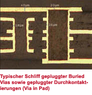
In the plugged holes, we guarantee a sleeve thickness of at least 15 µm. This is sufficient to be able to guarantee reliable further processing of the printed circuit right through to soldering without cracking or delamination, as the sleeves are given extra protection by the resin filling. The evenness of the copper deposit and the roundness of the edges of the vias is continually monitored during the grinding process.
If a copper "lid" is put on the pads, a thickness of at least 10 µm is guaranteed. For fine tracks (<100 µm), the copper build up must then start from a correspondingly low base copper strength (5 µm or 12 µm). Cutting sections for analysis ensures that there are no bubbles in the plug and that the copper thickness is correct.
6. Summary
The use of hole plugging technology opens up numerous solutions to optimise the layout designer's design. This also significantly increases the processing reliability for complex SBU circuit boards. CONTAG can offer you a very reliable and reproducible version of this technology, naturally also as a rush service.
Talk to our sales team (+49 30 351 788 - 0 or team
 contag.de). We will look together for a functional, optimised and cost-effective solution for your printed circuit boards.
For more detailed technological questions on printed circuit boards, please contact our CONTAG-team (+49 30 351 788 - 300 or team@contag.de).
Version: A
Your personal contact
+49 30 351 788-333
teamcontag.de
Quick-Links
 Enquiry, Order
Products Multilayer HDI-SBU technology Contact
Enquiry, Order
Products Multilayer HDI-SBU technology Contact